Thermal Pad vs Thermal Gap Filler vs Thermal Paste: Choosing the Right TIM
In most electronics thermal designs, engineers focus on the cold plate, the heatsink, or the airflow — and treat the thermal interface material (TIM) as a commodity. That is usually where the design fails. The TIM is the bottleneck between the heat source and the dissipation structure: a 100 W/m·K aluminium heatsink delivers nothing if a 0.3 mm air gap or a poorly chosen pad sits between it and the die. This guide compares the three main TIM families — thermal pads, gap fillers and thermal paste — and gives a simple decision logic to pick the right one for a given assembly.
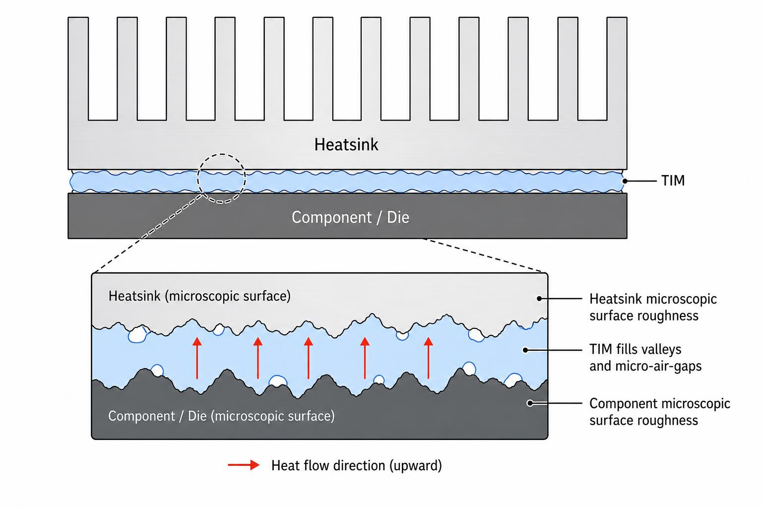
01 — Why thermal interface materials matter
Two metal surfaces that look perfectly flat are not. At the microscopic scale, real contact area is typically 1–2% of the apparent surface — the rest is air trapped in micro-roughness. Air has a thermal conductivity of about 0.026 W/m·K, three orders of magnitude below aluminium. A TIM replaces that air with a conformable material that wets both surfaces, fills the micro-irregularities and collapses the contact resistance.
The realized interface thermal resistance is rarely the bulk datasheet conductivity divided by thickness — interface contact resistance on both faces often dominates for thin layers. See Overheating in compact electronics for why this matters at the system level, and Cold Plates — The Ultimate Guide for the dissipation structures the TIM connects to.
02 — Thermal pads
Pre-formed elastomeric sheets — typically silicone loaded with ceramic, boron nitride or graphite particles — die-cut to the component footprint and placed dry between the heat source and the heatsink or enclosure.
Pros
- ›Clean, dry handling — no mess, no curing time
- ›Repositionable during assembly
- ›Consistent thickness, ideal for automated placement
Limits
- ›Higher contact resistance than paste at equivalent thickness
- ›Fixed thickness — cannot adapt to large tolerance variations
- ›Some loss of compression set over thermal cycling
Use cases
- ›Multiple components at varying heights on the same heatsink
- ›High-volume production where dispensing equipment is not justified
- ›Reworkable assemblies (service swaps, validation builds)
03 — Thermal gap fillers
Softer than pads, often two-component liquid systems dispensed onto the substrate and cured in place — or supplied as ultra-low-hardness pre-cured pads. Designed to absorb large gap variations without applying significant counter-force on the components.
Pros
- ›High conformability — fills irregular and non-parallel surfaces
- ›Absorbs mechanical tolerance stack-up across multiple components
- ›Low compression force, protecting fragile PCBs and packages
Limits
- ›Dispensing requires dosing control (volume, pattern, speed)
- ›Cure time and equipment cost for two-component systems
- ›Rework is harder than with pads — cured material adheres to both surfaces
Use cases
- ›EV / energy storage battery packs (cell-to-coldplate)
- ›Power modules with significant Z-axis tolerance stack-up
- ›Sensor and camera modules requiring low-stress assembly
04 — Thermal paste (grease)
Viscous, non-curing compounds — silicone or hydrocarbon based, loaded with metal oxides, boron nitride, silver or even liquid metal. Applied in very thin layers between two rigid, flat, well-mated surfaces. Delivers the lowest interface thermal resistance of the three families, at the cost of zero gap-filling capability.
Pros
- ›Lowest interface thermal resistance for flat, rigid contacts
- ›Very thin BLT — ideal where every micron of stack-up matters
- ›No mechanical pre-load constraint beyond surface mating
Limits
- ›Pump-out under thermal cycling — paste migrates out of the interface
- ›Dry-out and hardening over years, especially at high temperature
- ›No gap-filling capability — useless on uneven or non-parallel surfaces
- ›Application messy, hard to automate at scale, hard to rework cleanly
Use cases
- ›CPU / GPU dies bonded to a polished heatsink or vapor chamber
- ›High power-density semiconductors (IGBTs, MOSFETs) with controlled flatness
- ›Prototype thermal validation where a thin, defined BLT is required
05 — How to choose the right TIM
No TIM is universally best. The right choice falls out of four design parameters:
- Assembly tolerance. Fixed and flat (≤ 100 µm) → paste. Moderate and consistent (0.2 – 2 mm) → pad. Variable or large (≥ 1 mm with stack-up) → gap filler.
- Power dissipation / target Rth. Very low Rth needed (high-power CPU, laser diode) → high-k paste. Moderate power on multiple components → mid-range pad.
- Production constraints. Series production with placement robot → die-cut pad. Automated dispensing line available → gap filler. Prototype or low volume → pad or paste.
- Environment & lifetime. Vibration, long lifetime, wide temperature range → pad or cured gap filler (avoid paste pump-out). Controlled environment, short or refurbishable life → paste acceptable.
06 — Common mistakes when selecting a TIM
- ✗Underestimating the actual bond line thickness (BLT) once the assembly is closed — the gap in the CAD is rarely the gap in the prototype.
- ✗Confusing bulk thermal conductivity (W/m·K) with realized interface thermal resistance (K·cm²/W). Contact resistance dominates for thin layers.
- ✗Ignoring the available contact pressure — a hard pad in a low-force assembly never reaches its rated performance.
- ✗Overlooking long-term aging: pump-out for pastes, compression set for pads, dry-out for silicones in hot environments.
- ✗Specifying a high-k paste on surfaces that are not flat or rigid — performance collapses to worse than a basic pad.
- ✗Neglecting the surface treatment on the heatsink side — see Surtec 650 vs Anodizing for how coatings affect thermal contact.
07 — Related topics
08 — FAQ
Need help selecting and validating a TIM for your design? Reach out directly: